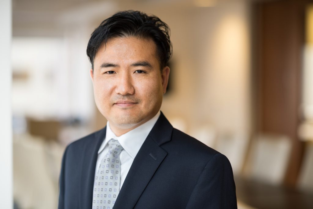
Overview
민 박사는 청정 기술, 전자·반도체 및 나노 기술 분야의 특허 준비 자문 및 소송에 초점을 맞춘 지적재산권 법률 전문가입니다.
로스쿨 진학 전 Intel Corporation에서 프로세스 통합 엔지니어, 나노 기술 전문가, 첨단 메모리 연구원 직을 역임했습니다. 민 박사는 Intel Corp.와 Micron Technology의 업계 최고 20nm NAND 플래시 기술 개발의 핵심 공헌자였으며, 이들 기업들은 이 기술로 최고의 권위를 지닌 UBM Techinsights가 수여하는 “2012년 올해의 반도체 상“을 수상했습니다. 민 박사는 14건의 특허를 보유하고 있으며 19편의 저널 간행물을 저술했습니다.
민 박사는 Si 기반 발광 나노 구조 및 장치에 관한 연구 논문으로 CALTECH(California Institute of Technology)에서 재료과학 박사 학위를 취득했습니다.
학력
- Santa Clara University(JD 학위, 2012), 우등생 명단(Dean’s List)
- California Institute of Technology(재료과학 박사, 1999), 인텔 펠로우십
- University of California – Los Angeles(재료과학 및 공학 이학사, 1994), U.C. Regents 장학금, 우등졸업(Cum laude)
Kyu Min, Ph.D. practices intellectual property law, with a focus on strategic patent protection and portfolio management, intellectual property due diligence and general counseling on infringement, licensing, international IP protection and post-grant proceedings. Kyu represents clients in the fields of advanced semiconductor devices and processing, metallurgy and materials science, energy storage devices and systems, optical displays and devices, medical diagnostics, clean technology, and nanotechnology.
Before attending law school, he worked as a process integration engineer, nanotechnologist, and advanced memory research technologist for Intel Corporation. Kyu was a key contributor in the development of the industry-leading 20 nm NAND flash technology by Intel Corp. and Micron Technology, for which the companies were awarded the prestigious Semiconductor of the Year Award in 2012 by UBM Techinsights. He holds fourteen patents and has authored nineteen journal publications.
Kyu received his Doctor of Philosophy in Materials Science from California Institute of Technology for his thesis research on Si-based light emitting nanostructures and devices.
Education
- Santa Clara University School of Law (J.D., 2012), Dean's List
- California Institute of Technology (Ph.D. Materials Science, 1999), Intel Fellowship
- University of California - Los Angeles (UCLA) (B.S. Materials Science & Engineering, 1994), cum laude, U.C. Regents Scholarship
Recognition
Awards & Honors
- Recognized by The Legal 500 “United States” for Patent Prosecution (2021)
Affiliations
- Institute of Electrical and Electronics Engineers (IEEE) Senior Member
News & Insights
Articles
“Time-Resolved Programming Current Measurement and Modeling for NAND-type Nanodot Flash Cell,”Chun-Chen Yeh, Karl Holtzclaw, Nirmal Ramaswamy, Srivardhan Gowda, Rhett Brewer, Thomas Graettinger, Kyu Min, Chandra Mouli, Krishna Parat, and T. P. Ma, IEEE Electron Device Lett. 29, 778-780 (2008).
“Frenkel-Poole trap energy extraction of atomic layer deposited Al2O3 and HfxAlyO thin films”, Chun-Chen Yeh, T.P. Ma, Nirmal Ramaswamy, Noel Rocklein, Dan Gealy, Thomas Graettinger, and Kyu Min, Appl. Phys. Lett. 91, 113521-113521 (2007).
“Void-mediated formation of Sn quantum dots in a Si matrix,” Y.Lei, P. Mock, T. Topuria, N. D. Browning, Regina Ragan, Kyu S. Min, Harry A. Atwater, Appl. Phys. Lett. 82, 4262-4264 (2003).
“Enhanced Exciton-Phonon Coupling in Spherical GaAs Nanocrystals Studied by Selective Excitation Spectroscopy,” Yoshihiko Kanemitsu, K. Masuda, Hiroshi Tanaka, M. Ando, Takashi Kushida, Kyu S. Min, and Harry A. Atwater, phys. stat. sol. (a) 190, 529–532 (2002).
“Direct energy gap group IV semiconductor alloys and quantum dot arrays in SnxGe1−x/Ge and SnxSi1−x/Si alloy systems,” Regina Ragan, Kyu S. Min, Harry A. Atwater, Materials Science and Engineering B 87 204–213 (2001).
“Visible light emission from GaAs nanocrystals in SiO2 films fabricated by sequential ion implantation,” Yoshihiko Kanemitsu, Hiroshi Tanaka, Yunosuke Fukunishi, Takashi Kushida, Kyu S. Min, and Harry A. Atwater, Phys. Rev. B 62 5100-5108 (2000).
“Size-dependent electron-hole exchange interaction in Si nanocrystals,” Mark L. Brongersma, Pieter G. Kik, Albert Polman, Kyu S. Min, and Harry A. Atwater, Appl. Phys. Lett. 76, 351-353 (2000).
“GaAs nanocrystals fabricated by sequential ion implantation: structural and luminescence properties,” Yoshihiko Kanemitsu, Hiroshi Tanaka, Takashi Kushida, Kyu S. Min, Harry A. Atwater, Physica E 7 322-325 (2000).
“Depth distribution of luminescent Si nanocrystals in Si implanted SiO2 films on Si,” Mark L. Brongersma, Albert Polman, Kyu S. Min, and Harry A. Atwater, J. Appl. Phys. 86, 759-763 (1999).
“A near-infrared photoluminescence study of GaAs nanocrystals in SiO2 films formed by sequential ion implantation,” Yoshihiko Kanemitsu, Hiroshi Tanaka, Takashi Kushida, Kyu Sung Min, and Harry A. Atwater, J. of Appl. Phys. 86 1762-1764 (1999).
“Tuning the emission wavelength of Si nanocrystals in SiO2 by oxidation,” Mark L. Brongersma, Albert Polman, Kyu S. Min, Elizabeth Boer, T. Tambo, and Harry A. Atwater, Appl. Phys. Lett. 72, 2577-2579 (1998).
“Photoluminescence from GaAs nanocrystals fabricated by Ga+ and As+ co-implantation into SiO2 matrices,” Shinji Okamoto, Yoshihiko Kanemitsu, Kyu S. Min, and Harry A. Atwater, Appl. Phys. Lett. 73, 1829-1831 (1998).
“Ultrathin pseudomorphic Sn/Si and SnxSi1-x/Si heterostructures,” Kyu S. Min and Harry A. Atwater, Appl. Phys. Lett. 72, 1884-1886 (1998).
“The role of quantum-confined excitons vs defects in the visible luminescence of SiO2 films containing Ge nanocrystals,” Kyu S. Min, Kirill V. Shcheglov, C. M. Yang, Harry A. Atwater, Mark L. Brongersma, and Albert Polman, Appl. Phys. Lett. 68, 2511-2513 (1996).
“Defect-related versus excitonic visible light emission from ion beam synthesized Si nanocrystals in SiO2,” Kyu S. Min, Kirill V. Shcheglov, C. M. Yang, Harry A. Atwater, Mark L. Brongersma, and Albert Polman, Appl. Phys. Lett. 69, 2033-2035 (1996).
“A small-specimen investigation of the fracture toughness of Ti5Si3,” K.S. Min, A.J. Ardell, S.J. Eck, and F.C. Chen, J. Mat. Sci., 30, 5479-5483 (1995).
“Endohedral rare-earth fullerene complexes,” E.G. Gillan, C. Yeretzian, K.S. Min, M.M. Alvarez, R.L. Whetten and R.B. Kaner, J. Phys. Chem., 96, 6869-6872 (1992).
“Collisional probes and possible structures of La2C80,” C. Yeretzian, K. Hansen, M.M. Alvarez, K.S. Min, E.G. Gillan, K. Holczer, R.B. Kaner and R.L. Whetten, Chem. Phys. Lett., 196, 337-342 (1992).
“La2C80: a soluble dimetallofullerene,” M.M. Alvarez, E.G. Gillan, K. Holczer, R.B. Kaner, K.S. Min and R.L. Whetten, J. Phys. Chem., 95, 10561-10563 (1991).
